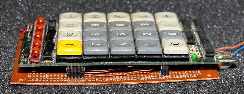
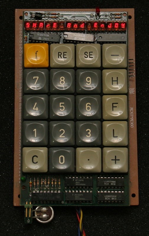
An old keypad & display module
The device
This all started with Traian (a ham friend of mine) receiving some of these devices as a gift. The original idea was to use just the keys, maybe even on a different PCB. However since I liked the display so much I managed to convince him to at least let me have the display units. Eventually he agreed to part with the whole devices intact. It seems that they were prepared as spares or in any case not really ready to use devices, as they lack the connectors. Or the connectors would plug into the metalized holes?
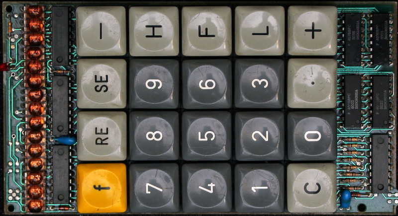
These seem to have been part of a logic tester of some kind. The H, F, L keys seem to indicate HIGH, FLOATING, LOW; + & - would set some polarity or maybe next/previous, RE & SE are RESET & SET, f is function. Apart from these assumptions I know nothing more.
Having the whole modules in my possession, I start thinking about reviving them in their present form. However, it's not yet clear what this is able to do by itself. It's not too difficult to identify where power should be applied, as to the voltage, most parts are CMOS 4000 series and the bypass capacitor is marked 10v, so 5v seems a safe bet. The use of CMOS ICs could mean a higher voltage, but there was nothing to indicate such a requirement.
Cautiously applying (current limited) power seems to do nothing. Everything remains dark, but on the bright side the power consumption is in mA range so there shouldn't be any smoke trouble ahead. There is no obvious oscillator on board so the lack of visible activity is not surprising.
Investigation
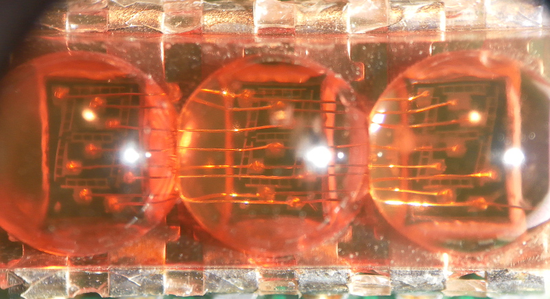
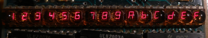
The display elements have small molded lens in front, and are packed in groups of three in a 12pin DIP package. They are soldered at an angle (the upper part is rised), I assume for better viewing. The lens diameter is 5mm and symbol height seems under 3 mm. I did not unsolder any display element to check for markings.
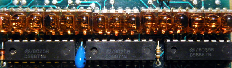
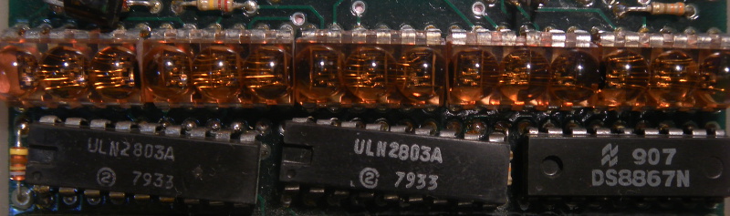
There are 3 similar boards, with one interesting difference. Two of them have been modified (note the skewed ULN2803s). The design seemed to call for DS8871N parts, but 2 boards were populated with (not pin compatible, thus the skew) ULN2803s.
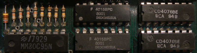
The IC list:
- 2 ULN2803A (array of 8 Darlington transistor pairs, typical driver) or DS8871N
- 1 DS8867N
- 1 MM80C95N
- 2 4015 (dual 4 bit shift register)
- 2 4076 (3-state 4 bit register)
- DS8867 - 8 segment constant current driver
- MM80C95N - 3-state hex buffer (non-inverting)
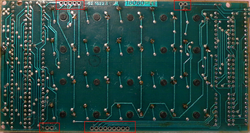
Mapping the connectors
After some trace following and continuity buzzing, the following map emerged
        +-----------------------------+
        |      TOP (DISPLAY)          |
        |                             |
        |o -> NC?                     |
        |o -> LED                    o| BUZZER (thru 2803)
        |                            o| CLOCK (common)
        |                            o| /KSEL (DS2)
     D7 |o-\                         o| /KSEL (DS1)
     D6 |o  } 4076 data in           o| DATA in (4015)
     D5 |o /                          |
     D4 |o/                           |
     D3 |o-\                          |
     D2 |o  } 4076 in & 80C95 out     |
     D1 |o /                          |
     D0 |o/                           |
    RST |o -> RST 4015 (all)          |
        |                             |
        |                             |
        |                            o| Vss
        |                            o| Vdd
        |                             |
        |                             |
        |                             |
        +-------------------------+ +-+
                                  |#| buzzer out -(from 2803)
                                  |#| buzzer out +(Vdd)
                                  +-+
Modus operandi
Now the pieces begin to fit together. The 4015 are cascaded and their outputs are used to sweep the display cathodes (select the current digit) and the row of keypad to be read (more about keypad below). CLOCK is connected directly to all clock inputs (1 for each 4076, and 2 on each 4015). Each sweep has 16 CLOCKs, but the first cycle doesn't seem to address any display or keyboard elements (Q1 of first shift register seems not connected). Digits are swept left to right with the 2803s driving the (common) cathodes for each digit and the DS8867 driving the anodes (segments).
At first CLOCK cycle of the sweep DATA is held HIGH before CLOCK is raised and lowered along with it. For all subsequent cycles DATA stays LOW, but D0-D7 must be set for the current digit to be displayed before CLOCK is raised (D0-D6 = segments A-G; D7 = decimal point; positive logic).
The keypad rows are tied (through 10K resistors) to the shift registers outputs - Q2-4 from the first and Q1-2 from the second. The keypad columns are weakly pulled to GND (100k resistors) and tied to 4 inputs of the MM80C95. It seems that the keypad is swept alongside with the display and read through the 80C95.
After these deductions, I started building something to test them. Since I always have a few PIC 16F1939 (useful for its reasonable speed, 5v operation and large number of I/O pins), this was to be used as controller. PORTB is used for D0-D7, 4 pins of PORTC (0-3) for CLOCK, /KSEL1&2, DATA and PORTD(7) for RST. The PIC is running at 4MHz using its internal RC oscillator (there is no need for crystal precision). Soldering the connectors was somewhat difficult because one side of the holes is covered by the keys. As usual, a serial (TTL) connector was included for outside control.
The software
The display sweep and keypad reading is done on a timer interrupt. The interrupt routine does everything related to display sweep and keypad reading, but relies on having a buffer filled with the data to output on D0-D7. The actual character "drawing" is done outside this routine. Also keypad data is loaded into a memory location (register, in PIC parlance) with column on the low nibble and row on the high one. This means "user" code doesn't have nice continuous scancode data (e.g. for a table read), but moves complexity out of interrupt code.
; INTERRUPT ROUTINE
        ORG 4
        CLRF    PCLATH  	; avoid GOTO/CALL landing in higher program memory if PCLATH points there
        BANKSEL PORTB		; ensure we're in the right BANK for data memory operations
        BTFSC   PIR3,TMR6IF
        GOTO    ONTMR6
; no other interrupts can occur for now
        GOTO    EOIE
; the code above for selecting the interrupt source is not useful at present
; but more interrupt sources could be used in the future
ONTMR6
        BCF     PIR3,TMR6IF	; clear interrupt flag
        CLRF    FSR0H		; clear HIGH BYTE of indirect register acces

        INCF    CRT_POS,F	; INCrement CRT_POS
        MOVF    CRT_POS,W
        SUBLW   0x0f
        BTFSC   STATUS,C	; if > 0x0f..
            GOTO    CRT_POS_NOT0
            CLRF    CRT_POS     ; ..reset to position 0
            BSF     PORTC,PDATA ; SET DATA for first walking bit
; LASTK is used outside interrupt routine as key pressed
; READK is internal to the interrupt routine
            MOVF    LASTK,W
            ANDLW   B'01111111'
            SUBWF   READK,W	; compare lower 7 bits of READK and LASTK
            BTFSC   STATUS,Z
            GOTO    NO_KDIF
                MOVF    READK,W ; if different copy the new READK to LASTK and..
                MOVWF   LASTK
                BTFSS   STATUS,Z
                    BSF     LASTK,7	; ..set bit 7 only if LASTK != 0
NO_KDIF
            CLRF    READK	; clear READK for next sweep
            GOTO    NO_DISP	; on first cycle don't display anything

CRT_POS_NOT0			; normal display
        MOVLW   DISP_DATA-1	; since on CRT_POS 0 there is no display
        ADDWF   CRT_POS,W	; it's useless to waste a byte of RAM, so start at CRT_POS-1
        MOVWF   FSR0L
        MOVF    INDF0,W		; get current symbol from buffer
        MOVWF   PORTB		; and set PORTB pins

NO_DISP
        BSF     PORTC,PCLOCK    ; raise the clock
        CALL    DRTRN           ; keep it up (DRTRN = slight delay)
        CALL    DRTRN           ; for a while
        BCF     PORTC,PCLOCK	; lower the clock
        BCF     PORTC,PDATA	; lower DATA (if it's already low no problem; it's quicker than another condition)
        MOVF    CRT_POS,W
        BTFSC   STATUS,Z	; do nothing more if CRT_POS == 0
            GOTO    EOIE
        SUBLW   5		; or if it is over 5
        BTFSS   STATUS,C
            GOTO    EOIE
; begin key reading
        BANKSEL TRISB
        MOVLW   0xff
        MOVWF   TRISB		; switch PORTB to INPUT
        BANKSEL PORTB
        BCF     PORTC,KS1	; pull both KSEL pins DOWN
        BCF     PORTC,KS2
        NOP			; a small delay
        MOVF    PORTB,W		; then read
        ANDLW   0x0f		; only lower nibble
        BTFSC   STATUS,Z	; if any key present
        GOTO    NOKEYPRES
            IORWF   READK,F	; add it to current READK
            SWAPF   CRT_POS,W
            IORWF   READK,F	; record the current row in high nibble
NOKEYPRES
        BSF     PORTC,KS1	; raise both KSEL pins
        BSF     PORTC,KS2
        BANKSEL TRISB
        CLRF    TRISB		; return PORTB to OUTPUT
        BANKSEL PORTD
EOIE
        RETFIE

DRTRN				; 4 (instruction) cycles delay = 4uS at 4MHz
        RETURN
Please excuse strange indenting, branching by "SKIP" instead of conditional jumps makes it so
"User" code is quite simple - a continuous loop that checks for incoming serial data and keypad "events" (the latter by checking bit 7 of LASTK and resetting it once read). If a (new) keypad press is detected, it's converted to ASCII and sent on the serial interface. If it's a digit key or one of -,H,F,L,+,. keys it is loaded into the display buffer as a hexadecimal digit. "C" clears the display (and sends "C" on serial). The display buffer is right aligned "calculator style". The serial "commands" are one character only (no CR or LF required) and mainly for debug - loading the buffer, changing the timer frequency etc.
Big efforts for a trivial purpose
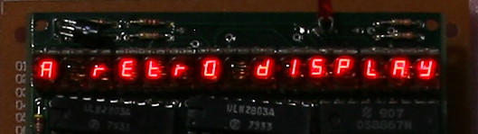
The story above happened some time ago (over a year). But recently, needing a logo for my retro stories, I thought that this would look good; however it was only able to display hexadecimal digits, not alphanumeric characters. Time for some modifications: added a new ASCII buffer and a function to convert ASCII to 7 segment - this would of course run into trouble with some letters: K,M,V,W but if those are avoided the result would not look bad at all.

My first idea was "retrocomputing" but because of the "M", I used "retro stories" for front page picture. I still don't know what else to use it for, yet. But should the occasion arise, it is ready for use.
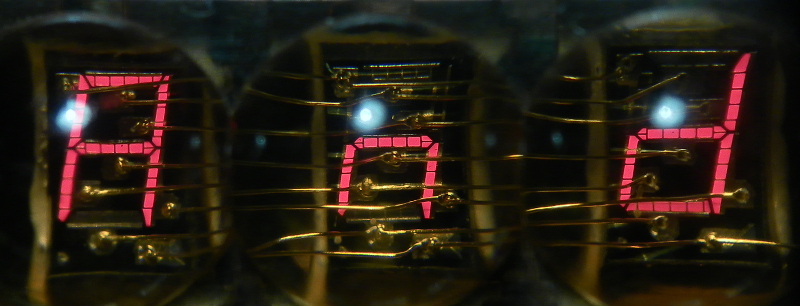
When writing this page I searched for the display elements using various descriptions and found them to be HP 5082-7433. The relevant page is at decadecounter.com. A datasheet is also available.
Published 2015-10-18 by Mihai Gaitos - contacthawk.ro